Product Summary
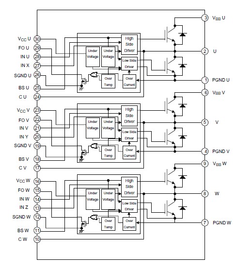
The MIG10J503H is an intelligent power module for three-phase inverter system. The 4th generation low saturation voltage trench gate IGBT and FRD of the MIG10J503H are connected to a three-phase full bridge type, and IC by the original high-voltage SOI(silicon-on-insulator) process drives these directly in response to a PWM signal. Moreover, since high-voltage level-shifter of the MIG10J503H is built in high-voltage IC, while being able to perform a direct drive without the interface with which the upper arm IGBT is insulated, the drive power supply of an upper arm can be driven with a bootstrap system, and the simplification of a system is possible. Furthermore, each lower arm emitter terminal of the MIG10J503H has been independent so that detection can perform current detection at the time of vector control by current detection resistance of a lower arm.
Parametrics
MIG10J503H absolute maximum ratings: (1)Collector-emitter voltage VCES: 600 V; (2)Each collector current (DC) IC: ±10 A; (3)Each collector current (PEAK) ICP: ±20 A; (4)Input voltage VIN: 5.5 V; (5)Fault output supply voltage VFO: 20 V; (6)Fault output current IFO: 15 mA; (7)PGND-SGND voltage difference VPGND-SGND: ±5 V; (8)Output voltage rate of change dv/dt: 20 kV/μs; (9)Collector power dissipation (per 1 IGBT chip) (Tc = 25℃)PC: 43 W; (10)Collector power dissipation (per 1 FRD chip) (Tc = 25℃)PC: 25 W; (11)Operating temperature TOPE: -20 to 100 ℃; (12)Junction temperature (Note 1) Tj: 150 ℃; (13)Storage temperature Tstg: -40 to 125 ℃; (14)Isolation voltage(60 Hz sinusoidal, AC)VISO: 2500 (1 min) Vrms; (15)Screw torque (M3): -0.5 N·m.
Features
MIG10J503H features: (1)The 4th generation trench gate thin wafer NPT IGBT is adopted; (2)FRD is built in; (3)The level shift circuit by high-voltage IC is built in; (4)The simplification of a high side driver power supply is possible by the bootstrap system; (5)Short circuit protection, over temperature protection, and the power supply under voltage protection function are built in; (6)Short circuit protection and over temperature protection state are outputted; (7)The lower arm emitter terminal has been independent by each phase for the purpose of the current detection at the time of vector control; (8)Low thermal resistance by adoption of original high thermal conduction resin.
Diagrams

 |
 MIG100J6CSB1W |
 Other |
 |
 Data Sheet |
 Negotiable |
|
||||
 |
 MIG100J7CSA0A |
 Other |
 |
 Data Sheet |
 Negotiable |
|
||||
 |
 MIG100J7CSB1W |
 Other |
 |
 Data Sheet |
 Negotiable |
|
||||
 |
 MIG100Q6CMA0X |
 Other |
 |
 Data Sheet |
 Negotiable |
|
||||
 |
 MIG100Q6CMB1X |
 Other |
 |
 Data Sheet |
 Negotiable |
|
||||
 |
 MIG10J503 |
 Other |
 |
 Data Sheet |
 Negotiable |
|
||||
 (China (Mainland))


